Semiconductor Equipment Stocks and Foundry Capex: Auditing Lithography Import Velocity, 10-Q Tool Deliveries, and DoD Microelectronics Commons Awards
The global semiconductor supply chain operates on a strict sequence of capital expenditure, physical tool delivery, and cleanroom qualification. Before a commercial fabrication facility produces a single operational wafer, equipment manufacturers must design, construct, transport, and calibrate specialized machinery. While market commentary frequently focuses on headline fab construction announcements and geopolitical subsidies, the true operational trajectory of chip manufacturing is documented in capital equipment order books, customs trade declarations, and federal prototyping task orders.
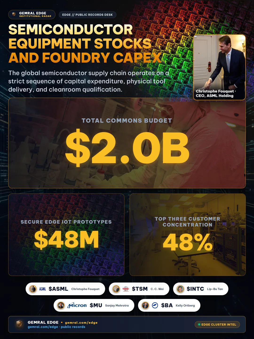
Semiconductor equipment stocks—anchored by ASML Holding (ASML), Applied Materials (AMAT), Lam Research (LRCX), and KLA Corporation (KLAC)—represent the capital goods foundation of global electronic production. These firms design the extreme ultraviolet lithography systems, atomic layer deposition chambers, high aspect ratio plasma etchers, and optical wafer metrology scanners required to fabricate transistors measured in single-digit nanometers. Public disclosures across SEC Form 10-Q filings, U.S. International Trade Commission import records under Harmonized Tariff Schedule Code 8486, and Department of Defense research awards reveal a clear multi-year capital convergence across commercial and national security sectors.
Foundry Capex Cycles: How Tool Delivery Lead Times Precede Commercial Fab Output
Capital deployment in semiconductor manufacturing follows an inflexible engineering timeline. Constructing an advanced cleanroom envelope requires 18 to 24 months of structural and environmental engineering. However, ordering, assembling, shipping, and installing frontline wafer fab equipment requires an additional 12 to 18 months of precision integration. Consequently, changes in equipment maker backlogs and delivery manifests precede actual factory volume output by more than a full calendar year.
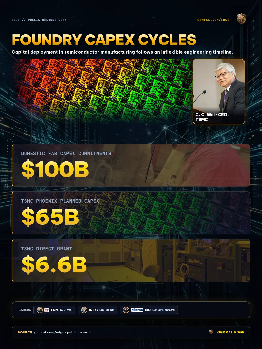
Consider the mega-fab buildouts initiated under the CHIPS and Science Act of 2022. Across the United States, commercial foundry operators committed over $100B in domestic manufacturing expansion. TSMC Fab 21 in Phoenix, Arizona, represents a planned investment of $65B across three distinct development phases, supported by $6.6B in direct federal grants and up to $5B in federal loans. Intel Foundry received an $8.5B direct funding award alongside $11B in federal credit facilities across 4 states, including New Albany, Ohio, and Hillsboro, Oregon. Samsung Electronics secured $6.4B in direct assistance for its Taylor, Texas fabrication complex, while Micron Technology finalized $6.1B for memory projects in New York and Idaho.
Despite public groundbreaking ceremonies dating back to 2022 and 2023, physical silicon production is dictated entirely by tool delivery schedules. A fab shell cannot process wafers until lithography steppers, chemical vapor deposition reactors, and automated wafer transport tracks are pressurized, leveled, and certified. Tracking public quarterly capital expenditure line items in SEC Form 10-Q filings demonstrates that foundry capex ramps sharply during the tool delivery phase—when 70% to 80% of total facility capital is transferred to equipment vendors.
Lithography Import Velocity: Auditing HTS 8486 Customs Data and Port Shipments
To audit the physical arrival of manufacturing apparatus before corporate earnings calls disclose operational yields, institutional analysts monitor public customs manifests and international trade databases. The U.S. International Trade Commission and U.S. Customs and Border Protection catalog semiconductor capital equipment under Harmonized Tariff Schedule Code 8486: "Machines and apparatus of a kind used solely or principally for the manufacture of semiconductor boules or wafers, semiconductor devices, electronic integrated circuits or flat panel displays."
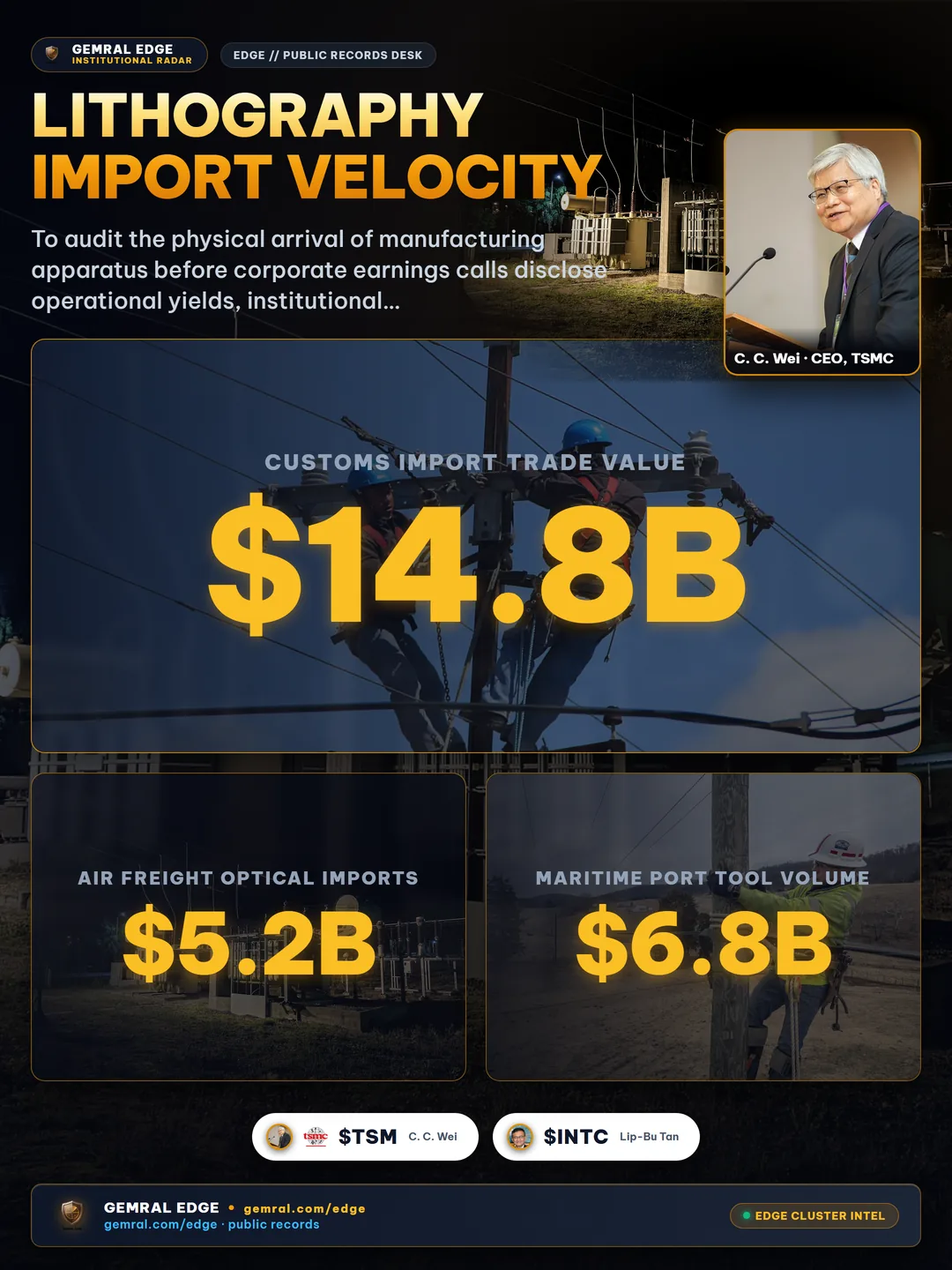
Subheading 8486.20 encompasses apparatus for the manufacture of semiconductor devices and integrated circuits, including photolithography steppers, dry etchers, and chemical vapor deposition chambers. Over the trailing 12 months, total U.S. import volume under HTS 8486 reached $14.8B. Dedicated air freight cargo through East Coast entry points accounted for $5.2B in sensitive optical and lithography modules, while West Coast maritime container ports received $6.8B in heavy wet-processing and automated handling machinery.
| Port of Entry | Transport Mode | Primary Equipment Category | Regional Destination |
|---|---|---|---|
| Port of Newark / JFK Airport | Air Freight & Maritime | EUV Optical Modules & Subsystems | Northeast Corridor / New York Fabs |
| Port of Los Angeles / Long Beach | Container Maritime | Robotic Wafer Handling & Wet Benches | Southwest Fabs (Arizona, New Mexico) |
| Dallas-Fort Worth (DFW) Airport | Charter Cargo Aircraft | Ion Implantation & Metrology Scanners | Texas Silicon Prairie (Austin, Taylor, Sherman) |
| Phoenix Sky Harbor (PHX) Cargo | Dedicated Cargo Freight | Lithography Systems & High-Purity Parts | TSMC Fab 21 & Intel Ocotillo |
Customs manifest tracking reveals that tool delivery volume peaked across Southwestern logistics nodes between Q4 2024 and Q3 2026. The clearance of specialized nitrogen-purged shipping containers coincides with cleanroom readiness milestones, providing empirical confirmation of equipment vendor revenue recognition under GAAP accounting rules.
DoD Microelectronics Commons: $269M in Prototyping Awards Across 8 Innovation Hubs
While commercial foundries focus on high-volume consumer and enterprise chips, the federal government has established a parallel procurement and prototyping network to ensure defense microelectronics supremacy. Authorized under the CHIPS and Science Act with a total program commitment of $2.0B across fiscal years 2023 through 2027, the Department of Defense launched the Microelectronics Commons, administered by the Naval Surface Warfare Center Crane Division (NSWC Crane) and the Strategic Technology Protection and Exploitation office.
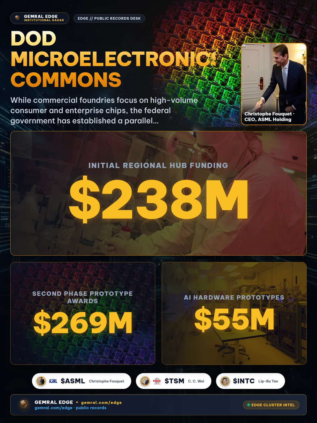
The program addresses the "lab-to-fab" transition—the persistent engineering gap where domestic laboratory research fails to transition into prototype production due to lack of access to commercial-grade fabrication tools. In September 2023, the DoD awarded $238M in Year 1 funding to establish 8 Regional Innovation Hubs spanning over 300 academic institutions, defense contractors, and semiconductor commercial entities. In September 2024, the Pentagon executed Year 2 project execution awards totaling $269M across 33 technical prototype task orders.
| Technology Area | Year 2 Funding | Prototype Projects | Primary Defense Applications |
|---|---|---|---|
| AI Hardware | $55M | 7 Projects | Autonomous edge computing, sensor fusion, low-power neural processors |
| Secure Edge / IoT | $48M | 6 Projects | Zero-trust telemetry, hardware root-of-trust, battlefield IoT sensors |
| Electromagnetic Warfare | $46M | 6 Projects | Gallium nitride (GaN) RF transmitters, radar signal processing, electronic jamming |
| 5G/6G Technology | $44M | 5 Projects | Millimeter-wave communications, tactical mesh networks, phased-array modules |
| Quantum Technology | $38M | 5 Projects | Cryogenic control circuitry, atom-trap sensors, quantum key distribution |
| Commercial Leap Ahead | $38M | 4 Projects | Silicon carbide (SiC) power switching, 3D heterogeneous packaging, photonic interconnects |
The allocation of $269M across these 33 prototype awards directs capital toward domestic semiconductor prototyping lines. To execute these defense task orders, participating research facilities and university cleanrooms are purchasing advanced deposition, etching, and metrology equipment, creating a durable secondary demand driver for tier-1 equipment manufacturers.
Tool Economics: From $380M High-NA Lithography to Sub-2nm Etch and Metrology Capex
The unit economics of frontline semiconductor capital equipment have escalated dramatically as feature dimensions shrink beneath 3 nanometers. Photolithography systems represent the single most expensive capital asset within any modern wafer fabrication facility.
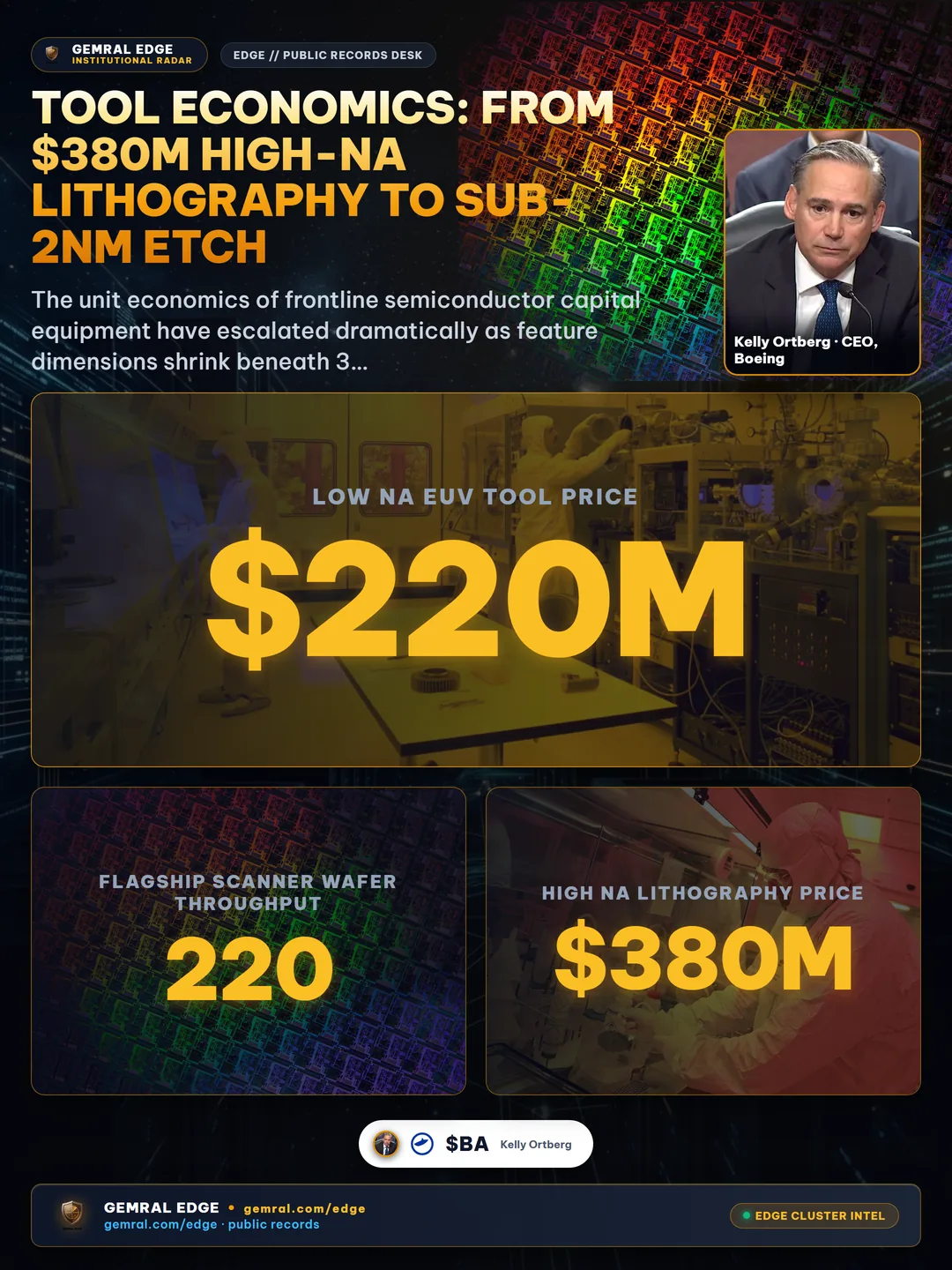
ASML holds an absolute commercial monopoly on Extreme Ultraviolet (EUV) lithography systems. Standard low-numerical-aperture EUV systems, such as the Twinscan NXE:3800B, command unit prices of approximately $220M. The NXE:3800B achieves a production throughput of 220 wafers per hour at a 30 millijoule exposure dose, representing a substantial throughput increase compared to the 160 wafers per hour achieved by the predecessor NXE:3600D.
For leading-edge sub-2nm fabrication and future Angstrom-era nodes, equipment economics enter an unprecedented tier. ASML developed High-Numerical-Aperture (High-NA) EUV systems featuring a 0.55 numerical aperture optical design capable of 8nm resolution. The High-NA Twinscan EXE:5000 and production-grade EXE:5200 carry price tags of approximately $380M per unit. The tool weighs over 150 metric tons and requires three dedicated Boeing 747 cargo flights to transport.
As gate-all-around (GAA) nanosheets replace FinFET transistor architectures, wafer fab equipment intensity expands. High aspect ratio etching and atomic layer deposition now represent over 30% of total cleanroom tool spending, while optical and electron-beam metrology intensity expands to 13.5% of total fab wafer fab equipment budgets.
To mitigate the extreme capital intensity of multiple EUV lithography exposures, equipment makers develop alternative materials engineering solutions. Applied Materials introduced the Centura Sculpta pattern-shaping system, designed to stretch patterned features along a single axis. Disclosed customer trial data indicates that implementing pattern shaping can eliminate one EUV double-patterning sequence, saving an estimated $250M in capital expenditure for every 100000 wafer-starts-per-month capacity in an advanced logic facility.
Equipment Maker Profiles: AMAT, ASML, LRCX, and KLAC Across the Fabrication Stack
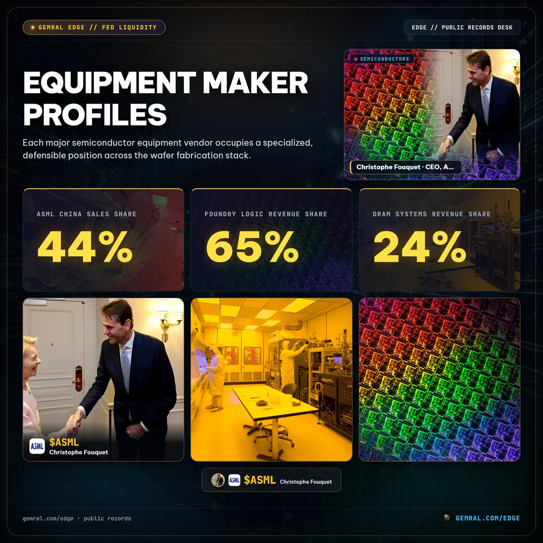
Each major semiconductor equipment vendor occupies a specialized, defensible position across the wafer fabrication stack. Evaluating these companies requires auditing product line concentration, customer exposure, and patent moats.
| Ticker | Company Name | Core Specialization | Revenue Concentration Profile |
|---|---|---|---|
| ASML | ASML Holding N.V. | EUV & DUV Photolithography | Monopoly in EUV; 44% China revenue share in recent quarters before curbs |
| AMAT | Applied Materials, Inc. | Deposition, Epi, Ion Implantation | 65% Foundry & Logic, 24% DRAM, 11% Flash memory systems |
| LRCX | Lam Research Corporation | High-Aspect-Ratio Etch & Clean | Leading supplier for 3D NAND vertical holes; top 3 customers drive 48% revenue |
| KLAC | KLA Corporation | Process Control & Yield Metrology | Over 50% global market share in wafer inspection; 13.5% fab capex capture |
ASML Holding (ASML): As the sole global supplier of EUV lithography systems, ASML acts as the ultimate gatekeeper for leading-edge silicon. The company's revenue recognition is tied to customer fab readiness. In recent quarters, mature-node deep ultraviolet (DUV) shipments to Chinese domestic foundries represented between 39% and 44% of total net system sales as regional chipmakers accelerated capital accumulation prior to expanded export licensing restrictions.
Applied Materials (AMAT): Operating the broadest portfolio in the equipment industry, Applied Materials captures value across nearly every process step outside of lithography. SEC Form 10-Q disclosures demonstrate that Foundry and Logic customers account for 65% of Semiconductor Systems revenue, with memory customers generating the remaining 35% (24% DRAM, 11% Flash). AMAT's integrated materials solutions allow chipmakers to co-optimize deposition, vacuum transfer, and surface treatment within single platform clusters.
Lam Research (LRCX): Lam Research dominates plasma etching and chemical vapor deposition processes. The company holds leadership in memory fabrication, particularly for 3D NAND flash structures where vertical channel holes must be etched through more than 300 alternating microscopic material layers with atomic precision. Public disclosures indicate that Lam's top 3 customers account for 48% of total gross revenue, creating high operational leverage to memory capital expenditure cycles.
KLA Corporation (KLAC): As chip structures shrink and defect tolerances approach zero, yield management becomes paramount. KLA Corporation maintains a dominant market share exceeding 50% in optical inspection and e-beam defect review. The company's Archer 750 overlay metrology and SpectraShape critical dimension platforms allow foundries to detect systemic yield excursions in real time, protecting hundreds of millions of dollars in work-in-progress silicon wafers.
Geopolitical Chokepoints: Export Control Bifurcation and Domestic Fab Buildout Delays
The semiconductor equipment industry operates at the intersection of international trade policy, technological sovereignty, and military readiness. Over the past 3 years, the U.S. Department of Commerce Bureau of Industry and Security (BIS), in coordination with Dutch and Japanese export authorities, enacted sweeping export restrictions targeting leading-edge semiconductor tooling.
These restrictions establish strict technical thresholds: advanced EUV lithography systems, sub-14nm logic etching tools, and memory manufacturing tools capable of producing DRAM beneath 18nm or NAND above 128 layers are prohibited from export to designated foreign entities without explicit government licensing. As evaluated in the Taiwan Strait & TSMC Semiconductor Shock Playbook, this policy has bifurcated global equipment demand into two distinct channels: leading-edge domestic expansion in the U.S., Europe, and allied Asian jurisdictions, versus intense mature-node (legacy 28nm, 45nm, and 65nm) capital accumulation in non-allied markets.
Simultaneously, domestic foundry projects funded by the CHIPS Act have encountered operational frictions. Complex cleanroom construction, specialized trade union labor requirements, and prolonged utility interconnection timelines have pushed back volume manufacturing schedules. TSMC rescheduled volume production of its 4nm process at Arizona Fab 21 from 2024 to early 2025, with its secondary 3nm/2nm cleanroom scheduled toward 2028. Intel restructured its manufacturing rollout timelines in Ohio, spacing out tool installations across multiple fiscal quarters.
For equipment vendors, these delays alter the cadence of revenue recognition under GAAP rules. Equipment makers typically record customer advance deposits upon purchase contract signing, but cannot recognize final system revenue until tools are delivered, assembled on-site, and pass final customer acceptance testing. Tracking deferred revenue balances in corporate 10-Q filings provides direct visibility into tool shipments awaiting final qualification sign-off.
How to Track Foundry Equipment Signals
Institutional analysis of semiconductor equipment stocks requires synthesizing independent public datasets rather than relying on sell-side earnings forecasts. To monitor capital cycles and execution timelines, market participants track four objective data streams:
- SEC Form 10-Q Tool Backlog and Deferred Revenue: Equipment makers report unfulfilled customer purchase orders and deferred revenue liabilities each quarter. A rising ratio of deferred revenue relative to recognized system sales signals that tools have shipped to fab cleanrooms but await final acceptance certification.
- Customs Import Manifests (HTS Code 8486): Tracking monthly import tonnage and declared values through U.S. ports of entry identifies when multi-million dollar lithography steppers and etching reactors arrive at regional fab clusters in Arizona, Texas, New York, and Ohio.
- Federal Research and Prototyping Task Orders: Public award bulletins from the DoD Microelectronics Commons and NSWC Crane disclose specific technology allocations (such as the $269M Year 2 awards across 33 prototypes), revealing which defense technologies are receiving direct hardware funding.
- Corporate 10-K Customer Concentration Disclosures: Auditing the percentage of revenue derived from leading foundries (TSMC, Samsung, Intel) reveals capital expenditure reallocations across commercial logic and memory segments.
By correlating customs arrival velocity with corporate balance sheet backlogs and federal prototyping awards—as demonstrated in our deep dives on GaN and SiC Power Semiconductor Subsystem Transition and Cross-Signal Alignment in Public Records—analysts establish an empirical perspective on the global semiconductor equipment cycle. As domestic fabrication facilities transition from construction frameworks into certified manufacturing environments, equipment vendors remain the foundational beneficiaries of global semiconductor capital investment.
Frequently asked questions
What are the leading semiconductor equipment stocks?
The primary tier-1 semiconductor equipment stocks are ASML Holding (ASML) for advanced photolithography, Applied Materials (AMAT) for materials engineering and deposition, Lam Research (LRCX) for high-aspect-ratio etching, and KLA Corporation (KLAC) for yield diagnostics and optical metrology.
How do equipment delivery lead times predict fab production?
Advanced wafer fab equipment requires 12 to 18 months from order placement to delivery, cleanroom installation, and baseline qualification. Tracking customs import manifests under HTS Code 8486 reveals equipment installation timelines well before commercial wafer output begins.
What is the DoD Microelectronics Commons program?
The Microelectronics Commons is a $2.0B initiative under the CHIPS and Science Act managed by NSWC Crane. It funded 8 regional innovation hubs with $238M in Year 1 and awarded $269M across 33 prototype projects in Year 2 to bridge laboratory research to domestic commercial fabs.
How expensive are cutting-edge semiconductor lithography tools?
Standard Low-NA EUV lithography systems such as the ASML Twinscan NXE:3800B cost approximately $220M each, while next-generation High-NA EUV systems (Twinscan EXE:5000 / EXE:5200) cost approximately $380M per unit.