GaN vs SiC: The Power Semiconductor Transition in High-Voltage AI Data Centers and EV Inverters
The global electrification transition across artificial intelligence data centers, commercial transport, and high-voltage power grids is colliding directly with the physical limits of traditional silicon. For more than five decades, silicon-based insulated-gate bipolar transistors (IGBTs) and metal-oxide-semiconductor field-effect transistors (MOSFETs) served as the primary switching engines of modern power conversion. However, as high-density AI clusters surpass 100 kW per rack and electric vehicles migrate to 800V architectures, legacy silicon dissipates excessive energy as parasitic heat. The resulting efficiency bottlenecks have sparked an accelerated migration toward wide-bandgap (WBG) compounds: Gallium Nitride (GaN) and Silicon Carbide (SiC).
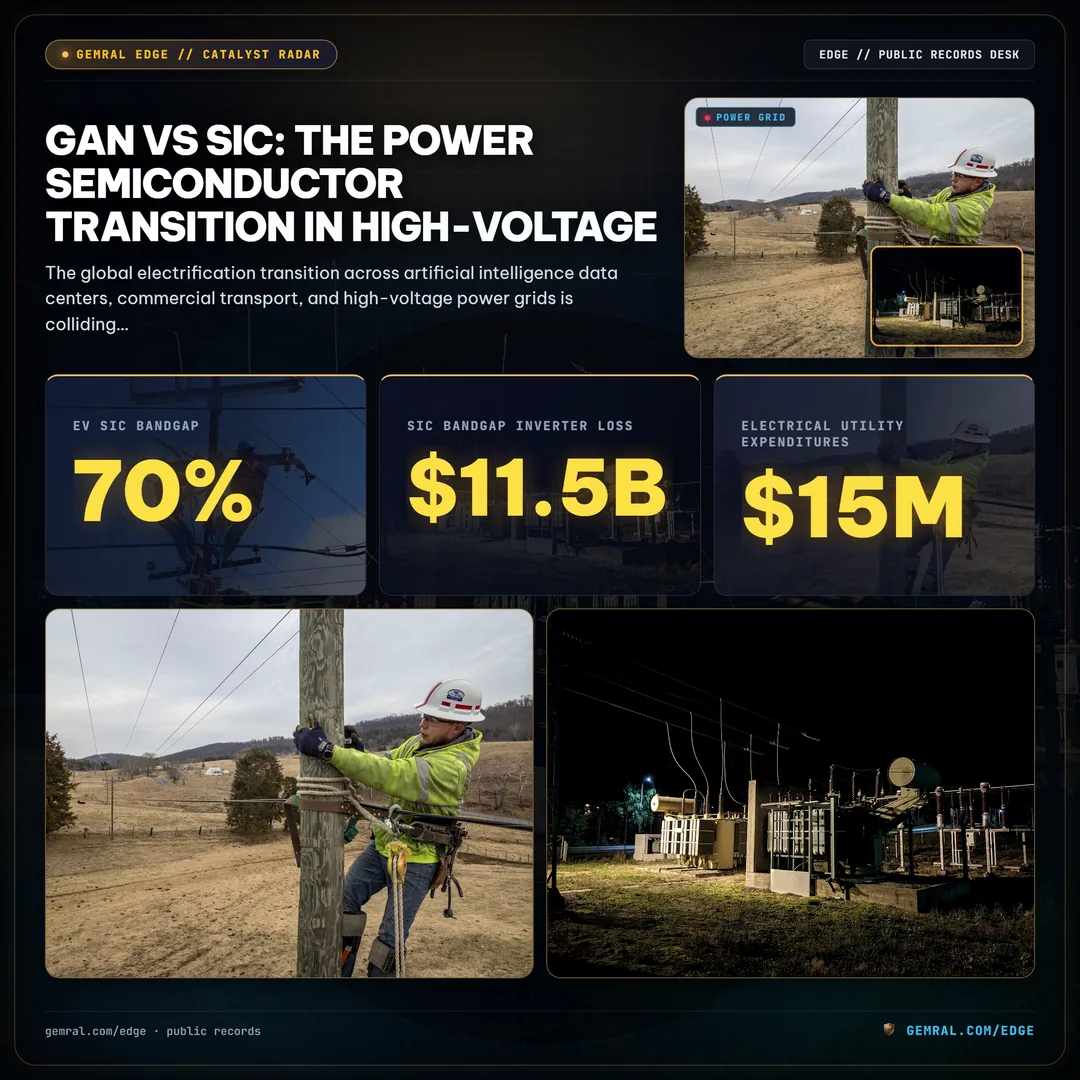
Understanding the battle between GaN vs SiC power semiconductors requires analyzing fundamental solid-state physics alongside industrial cost dynamics. While both materials dramatically outperform legacy silicon, they serve distinct operational domains rather than competing head-to-head across all applications. Engineers modeling high-efficiency powertrains utilize the GaN vs SiC inverter energy loss comparator to evaluate thermal dissipation tradeoffs across switching frequencies ranging from 20 kHz to 2 MHz. Public corporate filings and foundry supply chain disclosures reveal that SiC has secured dominance in high-voltage traction inverters, while GaN is capturing the high-frequency frontier inside hyperscaler server racks and modular energy storage units.
GaN vs SiC: Core Material Physics and Bandgap Divergence
The term "wide-bandgap" refers to the energy required to excite an electron from the top of the valence band to the bottom of the conduction band. In conventional silicon, this bandgap energy is 1.1 electron-volts (eV). By contrast, 4H-polytype Silicon Carbide exhibits a bandgap of 3.26 eV, while Gallium Nitride possesses a bandgap of 3.4 eV. This wider energy threshold allows both compound semiconductors to withstand electric breakdown fields approximately ten times greater than silicon—measuring 3.0 MV/cm for SiC and 3.3 MV/cm for GaN, compared to just 0.3 MV/cm for silicon.
Because the critical electric field is an order of magnitude higher, a wide-bandgap power transistor can support the same blocking voltage with an active drift layer that is roughly ten times thinner and doped an order of magnitude higher than a comparable silicon device. Consequently, the device's specific on-resistance (Rds(on) multiplied by active die area) drops by a factor of 100 to 300. Smaller die sizes translate directly into lower gate charge (Qg) and output capacitance (Coss), allowing transistors to switch states significantly faster with minimal capacitive discharge losses.
| Material Parameter | Silicon (Si) | Silicon Carbide (4H-SiC) | Gallium Nitride (GaN) |
|---|---|---|---|
| Bandgap Energy (eV) | 1.1 | 3.26 | 3.4 |
| Critical Breakdown Field (MV/cm) | 0.3 | 3.0 | 3.3 |
| Electron Mobility (cm²/V·s) | 1400 | 900 | 2000 (2DEG Channel) |
| Thermal Conductivity (W/m·K) | 1.5 | 4.9 | 1.3 |
| Saturation Velocity (10⁷ cm/s) | 1.0 | 2.0 | 2.5 |
| Dielectric Constant (Relative) | 11.8 | 9.7 | 8.9 |
Despite their shared wide-bandgap classification, GaN and SiC diverge sharply in two physical parameters: electron mobility and thermal conductivity. Gallium Nitride devices are constructed as High Electron Mobility Transistors (HEMTs), utilizing a two-dimensional electron gas (2DEG) formed at the hetero-interface of aluminum gallium nitride (AlGaN) and gallium nitride. Within this 2DEG quantum well, electrons move unimpeded by donor impurities, achieving an electron mobility of 2,000 cm²/V·s. This extreme mobility allows GaN to switch at multi-megahertz frequencies with near-zero reverse recovery charge (Qrr).
Conversely, Silicon Carbide boasts exceptional thermal conductivity of 4.9 W/m·K—more than triple that of silicon (1.5 W/m·K) and nearly four times that of GaN (1.3 W/m·K). This allows SiC power modules to evacuate heat efficiently from dense multi-chip packages, sustaining junction temperatures exceeding 175°C without thermal runaway. This thermodynamic divergence defines the natural boundary of their respective commercial applications.
Breakdown Voltage vs Switching Frequency: The Strategic Operational Divide
Power conversion systems operate across an engineering trade-off frontier defined by voltage rating, current carrying capacity, and switching frequency. When selecting power semiconductor components, design engineers map system topologies along this two-dimensional matrix. GaN dominates the high-frequency, low-to-mid voltage quadrant (80V to 650V, with emerging 900V variants), whereas SiC commands the high-voltage, high-current quadrant (650V to 1700V, extending up to 3.3 kV in traction and grid transmission).

In low-to-medium voltage environments, such as 48V telecom rectifiers, 400V microinverters, and consumer electronics chargers, switching frequency dictates passive component size. By operating at frequencies between 500 kHz and 5 MHz—ten to fifty times faster than silicon MOSFETs—GaN circuits reduce the required physical volume of magnetic inductors, chokes, and ceramic capacitors by up to 60%. The elimination of reverse recovery losses in GaN HEMT architectures enables bridgeless totem-pole power factor correction (PFC) topologies that deliver conversion efficiencies exceeding 99%.
However, above 650V to 900V, GaN encounters structural packaging and voltage isolation challenges. Commercial GaN transistors are lateral devices; high-voltage electric fields travel horizontally across the surface of the chip. Scaling lateral GaN devices to 1200V or 1700V requires substantial surface real estate, making the dies economically uncompetitive. By contrast, Silicon Carbide MOSFETs are vertical devices; current flows straight through the thickness of the wafer from the top source contact to the bottom drain metallization. This vertical architecture enables SiC to scale directly to 1200V, 1700V, and 3300V ratings while handling continuous currents exceeding 400 amperes per module.
If your application demands switching frequencies above 200 kHz at voltages under 650V—where magnetic downsizing and power density are paramount—GaN is the optimal technical choice. If your system operates at 800V to 1500V under heavy continuous thermal load—where bulk power throughput and passive heat dissipation dominate—SiC is the undisputed standard.
Hyperscaler AI Data Centers: 800V DC Power Architectures and Efficiency Gains
The rapid expansion of generative AI model training and real-time inference clusters has exposed severe electrical bottlenecks in modern data center infrastructure. Previous generations of enterprise server racks operated at power envelopes between 10 kW and 20 kW, utilizing standard 48V to 12V distributed power architectures. Modern AI accelerators—incorporating multi-die GPUs and custom application-specific integrated circuits (ASICs)—demand rack power densities reaching 40 kW, 80 kW, and even 120 kW per cabinet.

Distributing megawatts of power at legacy 48V DC requires heavy copper busbars measuring inches in thickness to carry thousands of amperes, introducing severe resistive I²R distribution losses. To mitigate these thermal losses, hyperscalers are transitioning toward 400V and 800V DC facility power distribution. In these high-density server architectures, power supply units (PSUs) must convert 480V three-phase alternating current into direct current with minimal energy waste.
| Power Supply Standard | Target Efficiency (50% Load) | Annual Loss per 100 MW Facility | Dominant Semiconductor Tech |
|---|---|---|---|
| 80 PLUS Gold | 92.0% | 8.0 MW Waste Heat | Legacy Silicon MOSFET / IGBT |
| 80 PLUS Platinum | 94.0% | 6.0 MW Waste Heat | Superjunction Silicon |
| 80 PLUS Titanium | 96.0% | 4.0 MW Waste Heat | Hybrid Silicon / SiC Diodes |
| Open Compute Titanium+ | 97.5% | 2.5 MW Waste Heat | GaN Bridgeless Totem-Pole PFC |
In a 100 MW hyperscaler campus, improving power supply efficiency from 94% (Platinum) to 97.5% (Titanium+) recovers 3.5 MW of continuous electricity. Over a standard five-year operating lifecycle, this conservation prevents over $15M in wasted electrical utility expenditures while eliminating the corresponding water and HVAC chilling burden required to cool the facility. As analyzed in our review of sovereign AI infrastructure and bilateral compute compacts, power interconnect constraints and gigawatt-scale data center buildouts are elevating high-efficiency power semiconductors into strategic national assets. Gallium Nitride devices enable power supply units delivering 100W/in³ volumetric power density—more than double the 45W/in³ achieved by silicon designs. This spatial compaction frees multiple rack units (U) of cabinet space, allowing cloud operators to deploy additional compute nodes within the same physical footprint.
Electric Vehicle Inverters and On-Board Chargers: 800V Powertrain Adoption
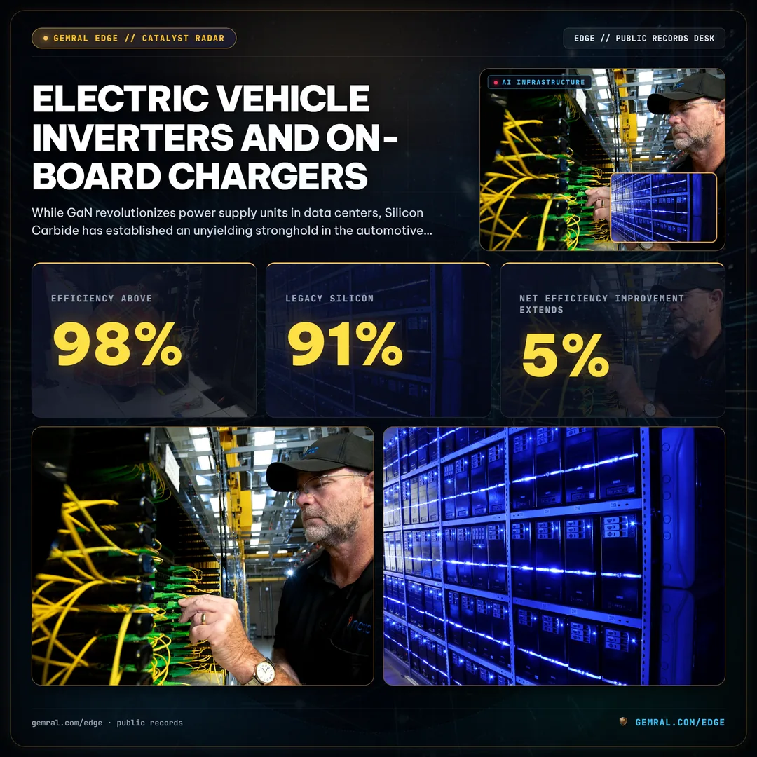
While GaN revolutionizes power supply units in data centers, Silicon Carbide has established an unyielding stronghold in the automotive powertrain. The primary propulsion inverter represents the second most critical component in an electric vehicle after the battery pack itself. It converts high-voltage direct current stored in the lithium-ion cells into three-phase alternating current to drive the traction motor.
Historically, electric vehicles utilized 400V battery architectures driven by silicon IGBTs. Silicon IGBTs suffer from an inherent physical limitation known as "tail current"—a lingering flow of minority carriers during turn-off that causes substantial switching energy loss. Because silicon inverters generate severe switching losses at higher frequencies, automotive engineers were forced to restrict inverter switching speeds to 8 kHz to 10 kHz, resulting in larger, heavier motor stator windings.
Silicon Carbide MOSFETs eliminate minority carrier tail currents entirely, enabling unipolar switching at 20 kHz to 50 kHz with a 70% reduction in dynamic power loss. In standard urban drive cycles, where electric vehicles operate primarily under light-to-moderate partial load conditions, SiC inverter efficiency remains above 98%, compared to 91% to 93% for legacy silicon. This 5% to 7% net efficiency improvement extends vehicle driving range by 25 to 40 miles on the same battery capacity, or alternatively allows automotive manufacturers to downsize battery packs by 4 kWh to 6 kWh while maintaining equivalent range, eliminating hundreds of dollars in raw pack cost.
Furthermore, the automotive industry's ongoing transition from 400V to 800V electrical architectures—led by platforms such as Porsche Taycan, Hyundai E-GMP, and next-generation commercial trucks—mandates switching devices rated for 1200V breakdown margins. At 1200V, silicon IGBT conduction losses spike dramatically, making Silicon Carbide the only commercially viable solution capable of supporting 350 kW ultra-fast DC charging profiles that replenish 80% battery capacity in under 18 minutes.
Thermal Conductivity and Packaging Challenges in Extreme Operating Envelopes
The superior electrical characteristics of wide-bandgap semiconductors create intense secondary engineering challenges in thermal management and device packaging. Because GaN and SiC dies are between one-third and one-fifth the surface area of equivalent silicon chips, heat generation is concentrated across microscopic junction footprints. A power device dissipating 100 watts across a 10 mm² die experiences five times the localized heat flux of a legacy 50 mm² silicon transistor.

Here, the profound thermal conductivity advantage of Silicon Carbide becomes apparent. With a thermal conductivity of 4.9 W/m·K, SiC functions almost as a solid heat conductor. Heat generated in the sub-micron channel conducts rapidly through the bulk crystalline substrate into the leadframe and copper baseplate. SiC power modules can sustain continuous junction temperatures (Tj) of 175°C, with specialized defense-grade modules qualified up to 200°C. This allows automotive designers to simplify liquid cooling loops, reduce radiator surface area, and employ ethylene-glycol coolant shared with the cabin climate system.
Gallium Nitride, with a modest thermal conductivity of 1.3 W/m·K, cannot dissipate high thermal flux through its bulk crystal. Furthermore, commercial GaN HEMTs are mounted on silicon substrates that have a thermal expansion mismatch with the epitaxial layers. To prevent catastrophic thermal degradation, packaging engineers utilize top-side cooling surface-mount device (SMD) packages, such as PQFN and TO-leadless (TOLL) formats. Top-side cooling allows heat sinks to attach directly to the exposed metal pad on the top of the package, bypassing the thermal resistance of the printed circuit board (PCB) and providing an unobstructed thermal path to chassis cold plates.
Wafer Slicing and Substrate Yield: The Cost Trajectory of Silicon Carbide vs GaN-on-Si
The ultimate determinant of market adoption speed between GaN and SiC is substrate manufacturing economics. Standard electronic-grade silicon is grown via the Czochralski method: high-purity silicon melts at 1,414°C and single-crystal ingots measuring 300 mm (12 inches) in diameter are pulled from the crucible within days at negligible raw material cost. Neither Silicon Carbide nor Gallium Nitride can be manufactured using this traditional melt-pulling approach.

Silicon Carbide boules must be grown through physical vapor transport (PVT) or sublimation at temperatures exceeding 2,200°C inside sealed graphite crucibles. The growth process is painfully slow, advancing at a rate of 0.5 mm to 2 mm per hour. The resulting crystalline boules are extremely hard—ranking 9.5 on the Mohs scale, just below diamond. Slicing these boules into thin 350-micron wafers requires diamond wire saws or laser slicing (such as DISCO or Infineon Cold Split), resulting in substantial kerf loss where nearly half the grown crystal is discarded as waste dust.
| Economic Attribute | Legacy Silicon (Si) | Silicon Carbide (SiC) | Gallium Nitride on Silicon (GaN-on-Si) |
|---|---|---|---|
| Primary Substrate Diameter | 300 mm (12-inch) | 150 mm transitioning to 200 mm | 150 mm & 200 mm (Standard Fabs) |
| Substrate Growth Method | Czochralski Melt (1,414°C) | Sublimation PVT (2,200°C) | MOCVD Epitaxy on Silicon Substrate |
| Relative Raw Wafer Cost | 1.0x (Baseline ~$40) | 20x - 30x ($800 - $1,200) | 3x - 5x ($120 - $200) |
| Wafer Defect Density | Extremely Low (<0.1 /cm²) | Moderate (Basal Plane Dislocations) | Lattice Mismatch Strain Controlled |
| Fab Infrastructure Reusability | Fully Depreciated | Dedicated High-Temp Fabs | Existing Depreciated Silicon CMOS Fabs |
Consequently, raw 150 mm SiC substrates command prices between $800 and $1,200 each. The industry is currently executing an aggressive transition toward 200 mm (8-inch) SiC wafer fabs—anchored by investments from Wolfspeed in Marcy, New York, STMicroelectronics in Catania, Sicily, and Onsemi in Bucheon, South Korea. Expanding wafer diameter from 150 mm to 200 mm increases the usable die count per wafer by approximately 85%, cutting the cost per net good die by 30% once manufacturing yields stabilize above 70%.
Gallium Nitride approaches the cost curve from an entirely different strategic angle. Instead of growing expensive native GaN boules, commercial manufacturers deposit an ultra-thin (3 to 5 micron) epitaxial stack of GaN onto standard, low-cost silicon wafers (GaN-on-Si) using Metal-Organic Chemical Vapor Deposition (MOCVD). Because the underlying substrate is inexpensive silicon, GaN devices can be fabricated in standard, fully depreciated 150 mm and 200 mm silicon CMOS fabs. This enables fabless and fab-lite semiconductor suppliers to scale production rapidly without billions in dedicated greenfield foundry capital, ensuring GaN's cost trajectory will approach parity with premium superjunction silicon over the next three to five years.
Industrial and Defense Electrification: High-Reliability Subsystem Transitions
Beyond commercial data centers and consumer passenger vehicles, wide-bandgap semiconductors are driving a profound architectural transition across heavy industrial, aerospace, and defense applications. In renewable energy infrastructure, utility-scale photovoltaic solar farms and grid-tied battery energy storage systems (BESS) are migrating from 1000V DC to 1500V DC bus standards. Operating at 1500V reduces current flow, cutting resistive copper transmission losses and enabling central inverters utilizing 1700V and 2300V SiC modules to achieve round-trip power conversion efficiencies exceeding 99.2%.
In aerospace and tactical defense applications, system mass and volumetric footprint carry a severe operational penalty. Traditional military radar transmitters, shipboard power converters, and unmanned aerial vehicle (UAV) motor drives relied on heavy, oil-cooled transformers and bulky silicon switches. Transitioning to Gallium Nitride active electronically scanned array (AESA) radar transceivers dramatically expands transmission range and multi-target tracking bandwidth while reducing front-end cooling equipment mass by half.
Similarly, naval propulsion systems and tactical microgrids deploy solid-state power substations powered by high-voltage Silicon Carbide MOSFETs. By switching directly at medium distribution voltages (4.16 kV to 13.8 kV), SiC solid-state transformers eliminate heavy low-frequency iron-core magnetic components, reducing power electronics subsystem volume by up to 70%. These subsystem shifts mirror the capital expenditure trends detailed in our analysis of semiconductor equipment stocks and foundry capex, where tool delivery lead times and dual-use packaging investments signal broad capacity expansion. As federal procurement mandates prioritize energy resilience and supply chain self-sufficiency, public capital commitments under the CHIPS Act and national defense prototyping initiatives are cementing wide-bandgap semiconductor manufacturing as a foundational pillar of modern industrial strategy.
Frequently asked questions
What is the primary difference between GaN and SiC semiconductors?
The primary operational difference lies in voltage threshold and switching frequency: GaN offers significantly higher electron mobility enabling megahertz-range switching at voltages up to 650V-900V, whereas SiC provides higher breakdown voltage (650V-3300V) and three times higher thermal conductivity for extreme power density.
Why are AI data centers adopting GaN power supplies?
Next-generation AI server racks consuming 40kW to 100kW+ require titanium-grade 97.5%+ power supply unit (PSU) efficiency. GaN enables power supplies operating at 100W/in³ power density, reducing conversion losses and freeing valuable cleanroom rack space for compute accelerators.
How does Silicon Carbide improve electric vehicle range?
Replacing traditional silicon IGBTs with SiC MOSFETs in 800V EV traction inverters reduces switching losses by up to 70%, translating directly into a 5% to 10% battery range extension and enabling 15-minute ultra-fast DC charging.
What is the manufacturing cost difference between GaN and SiC?
GaN devices are typically grown epitaxially on standard silicon substrates (GaN-on-Si), utilizing depreciated 150mm and 200mm silicon fab infrastructure. Conversely, SiC requires synthetic boule sublimation at over 2,000°C and diamond sawing, resulting in higher raw substrate costs.